
Semiconductor Package Market: Technology has transformed the Semiconductor Package Market in recent years. Our in-depth analysis report covers several aspects of the industry, including its size, current state, and prospects.
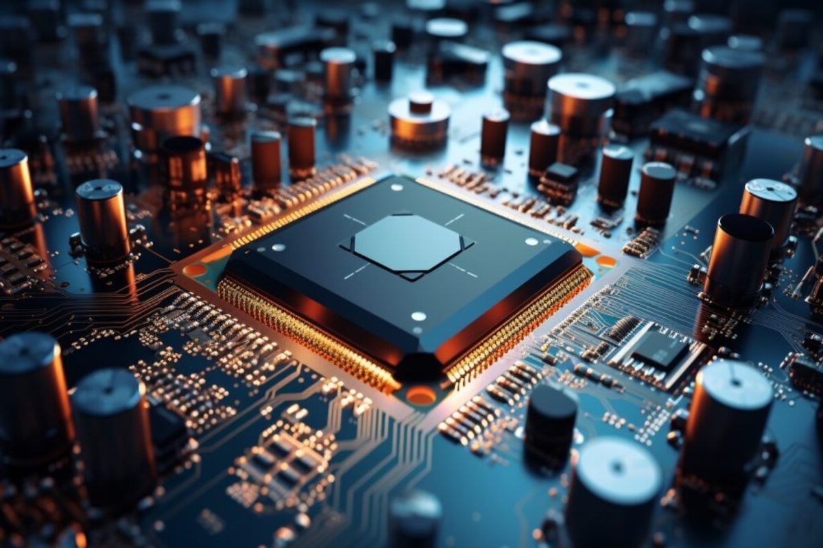
Advanced semiconductor packaging technologies have changed fast. SiP, WLP, and FOWLP have replaced wire bonding and flip-chip packaging. New packaging techniques promote integration, performance, and heat management. They work well with 5G, IoT, and AI, which are growing and evolving.
Our study also shows a bright future for semiconductor packaging due to the need for smaller, quicker, lower-power electronics. Self-driving technologies and EVs are pushing battery and sensor demand. This tendency is accelerating vehicle chip package growth.
Additionally, company mergers are becoming common. We are now putting various chips in one package. This will improve efficiency, energy savings, and speed. The sector also starts employing eco-friendly packaging and production practices. This fits the global search for better technology.
This tale shows how the market has developed in various countries and will continue to expand. It divides product type, use, and user type. Think seriously about the competition next. We must study industry leaders. Check their tactics, company, and future goals. The report shows the top creators’ market share.
This research may aid firms and smart investors. Understanding the semiconductor package industry helps them make smart selections. Stakeholders may plan for long-term success when they know much about growth, the market, consumers, competitors, and new developments.
Read More: Company Performance Reports: CPI, and Consumer Sentiment Index in Focus
The chip packaging business shows how technology advances. System-in-Package (SiP), Wafer-level packing (WLP), and Fan-out WLP have replaced wire bonding and flip-chip packing. This has sparked innovation. These clever methods and AIoT have changed how components are built, how things perform better, and how heat is regulated. This smart tweak benefits modern applications like 5G, IoT, and AI.
More than ever, electronic gadgets need tiny, quick, and low-power solutions. Because we require sensors and power units, chip packing has multiplied. Electric automobiles (EVs) and self-driving technologies are pushing demand for automotive chip packaging. These forces have changed the market.
Semiconductor packaging is changing drastically. It’ll spur industrial innovation. Combining items to make them better and use less energy is a huge trend. Mixing chips improves performance. It accelerates and improves. As the firm evolves, sustainability becomes crucial. Because it employs eco-friendly packing materials and manufacturing processes, semiconductor packaging supports global technological improvements.
This tale shows how the market has developed in various countries and will continue to expand. It divides product type, use, and user type. Next, consider the competition. We must investigate industrial giants. We must examine their tactics, company, and future goals. The report shows the top creators’ market share.
This research may aid firms and smart investors. Understanding the semiconductor package market aids decision-making. Stakeholders may prepare for long-term success by knowing how a market expands, what consumers want, how firms compare, and what’s new. As technology advances, semiconductor package markets shift. It’s like a fantastic symphony that shapes electronics.
Our Reader’s Queries
How big is the semiconductor packaging market?
The semiconductor packaging industry has been on a steady rise, with a current market size of USD 27.78 billion in 2022. Experts predict that this figure will soar to USD 65.46 billion by 2032, with a remarkable CAGR of 9% from 2023 to 2032. This growth is a testament to the increasing demand for semiconductor packaging solutions across various industries. As technology continues to advance, the need for efficient and reliable packaging solutions will only continue to grow.
What is packaging in semiconductor industry?
Semiconductor wafers are the foundation of integrated circuits that power much of today’s technology. To safeguard them from chemical contamination, light, heat, and impacts, they are packaged in metal, plastic, ceramic, or glass. This packaging also connects them to their surroundings.
What is package type of semiconductor?
There are two types of packages available – the through-hole mount PGA type and the surface mount BGA type. The PGA (Pin Grid Array) type is a through-hole mount package that features lead pins arranged in an array and mounted vertically on the bottom of the package, resembling a nailbrush.
Which countries are involved in semiconductor packaging?
The Semiconductor Chip Packaging Market is being led by North America, Europe, and Asia-Pacific regions. These regions include countries such as the United States, Canada, Mexico, Germany, UK, France, Italy, Russia, Turkey, China, Japan, Korea, India, Australia, Indonesia, Thailand, Philippines, Malaysia, and Vietnam.