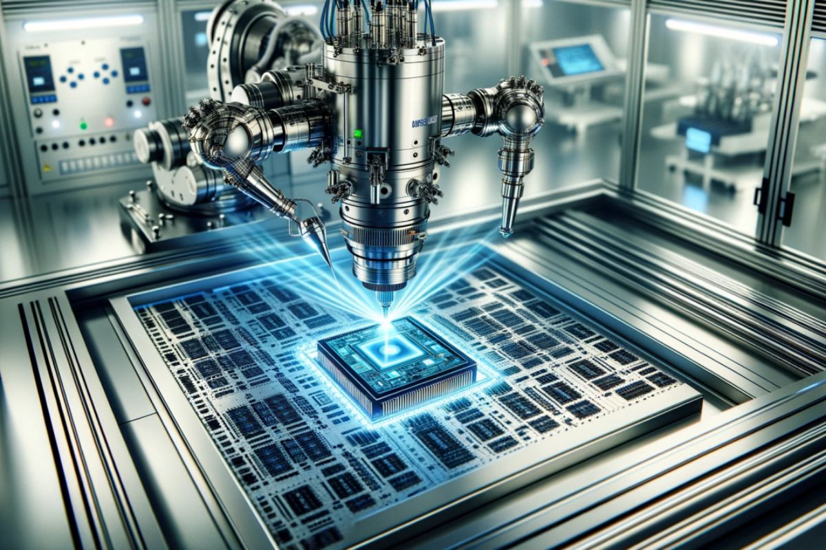
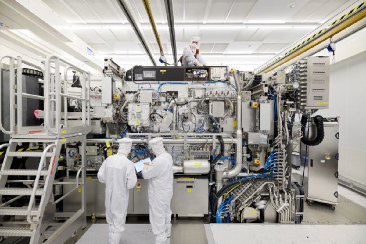
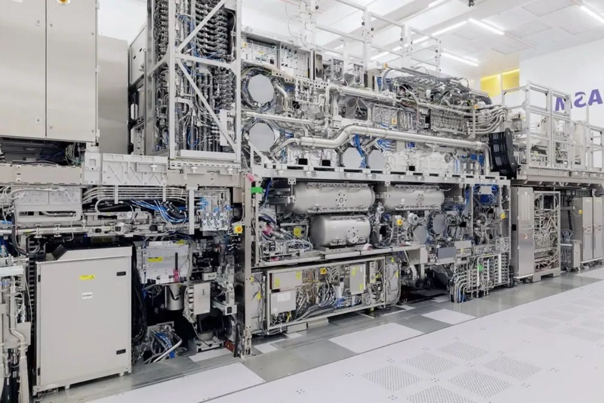
ASML’s Technological Leap: ASML, the Dutch semiconductor lithography giant, has set the stage for a monumental shift in chip manufacturing with its latest technological marvel, the High NA EUV machine. Promising unparalleled precision and efficiency, this cutting-edge system is poised to revolutionize the industry.
But as competitors scramble to catch up, the real question looms: Will this innovation solidify ASML’s dominance, or will it open the door to a new era of fierce competition and technological advancement? The implications of this unveiling are vast and could reshape the landscape of semiconductor manufacturing as we know it.
Key Takeaways
- Enhanced optics and advanced control systems boost performance and resolution.
- Industry cautiously optimistic about economic viability amid high costs.
- Major players like Intel, TSMC, and Samsung show interest in adopting technology.
- ASML’s High NA EUV Machine poised to revolutionize chip manufacturing processes.
ASML’s New High NA EUV Machine
With the unveiling of ASML’s new High NA EUV machine, the semiconductor industry braces itself for a technological revolution that promises to redefine the landscape of chip manufacturing. ASML’s $350 million investment in this cutting-edge device is a bold statement of intent, showcasing their commitment to staying at the forefront of the fiercely competitive semiconductor market.
Also Read: ASML Faces Export Freeze: U.S. Influence Prompts Dutch Government Action Against China Shipments
This High NA EUV machine is not just another tool in the arsenal of chipmakers; it represents a leap forward in lithography technology, enabling the production of smaller, more powerful chips with unparalleled precision and efficiency. ASML’s latest innovation is poised to set a new standard in chip manufacturing, solidifying their position as the undisputed leader in semiconductor equipment development.
Technical Details and Functionality of the High NA EUV Machine
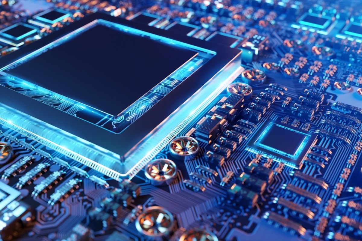
ASML’s High NA EUV machine epitomizes a quantum leap in semiconductor lithography technology, revolutionizing chip manufacturing with its enhanced optical system and unprecedented resolution capabilities. This cutting-edge machine boasts the following technical details and functionalities:
- Enhanced Optics: The High NA EUV machine features a larger optical system, allowing for the precise focusing of extreme ultraviolet light onto the silicon wafer.
- Increased Resolution: With improved resolution capabilities, this machine enables chipmakers to shrink the size of features on their chips by up to 40%, paving the way for more advanced and powerful semiconductor devices.
- Advanced Control Systems: Equipped with state-of-the-art control systems, the High NA EUV machine ensures unparalleled accuracy and consistency in chip manufacturing processes.
- Optimized Throughput: This machine is designed to optimize throughput, enhancing productivity and efficiency in semiconductor fabrication.
Market Adoption and Economic Viability
The future of market adoption and economic viability for ASML’s High NA EUV machine hangs in the balance, with analysts and industry players closely monitoring its trajectory towards widespread utilization.
ASML’s ambitious plans to ship multiple High NA EUV machines this year have sparked both excitement and skepticism in the semiconductor industry. While some chipmakers may be eager to embrace this cutting-edge technology for a competitive edge, the exorbitant costs associated with the High NA EUV machine could hinder its immediate uptake.
Experts suggest that broader adoption may not occur until the technology becomes more economically feasible, potentially not reaching a tipping point until around 2030-2031. The stakes are high as the industry navigates the delicate balance between innovation and financial viability in the race to revolutionize chip manufacturing.
Industry Response and Potential Impact on ASML’s Market Dominance
In the realm of semiconductor technology, ASML’s High NA EUV machine is poised to not just disrupt but dominate the market landscape, with industry giants like Intel, TSMC, and Samsung already signaling their intent to harness its revolutionary capabilities. This swift industry response is a testament to the groundbreaking nature of ASML’s technology and its potential to revolutionize chip manufacturing. The impact on ASML’s market dominance is palpable, with the following key points to consider:
- Intel’s Early Adoption: Intel’s reception of a pilot device showcases a strong commitment to integrating ASML’s High NA EUV machine into their manufacturing processes.
- TSMC and Samsung’s Intentions: Expressions of interest from TSMC and Samsung indicate a competitive shift towards ASML’s cutting-edge technology.
- ASML’s Production Goals: The ambitious target of delivering 20 machines annually by 2028 underscores ASML’s confidence in meeting market demand.
- Solidifying Market Dominance: The enthusiastic uptake of this technology could further cement ASML’s position as a dominant force in the lithography systems market.
Geopolitical Factors and ASML’s Business Outlook
Amidst global tensions and strategic intricacies, the interplay of geopolitical factors casts a shadow over ASML’s business outlook, shaping a narrative of uncertainty and opportunity in the semiconductor landscape.
Notably, ASML has faced restrictions on exporting its cutting-edge machines to China due to US regulations on advanced technology exports. Despite this hurdle, ASML’s robust order book and the immense potential for substantial sales and margin boosts paint a positive trajectory for the company.
With its High NA EUV machine poised to revolutionize the semiconductor industry, ASML stands at the brink of solidifying its position as a pivotal player in chip manufacturing technology.
The intricate dance of geopolitics adds complexity to ASML’s forecast, where challenges intertwine with lucrative prospects, creating a dynamic landscape for the semiconductor giant.
Conclusion Of ASML’s Technological Leap
ASML’s unveiling of the high NA EUV machine marks a revolutionary leap in chip manufacturing technology. With its advanced capabilities and potential to transform the industry, this new machine is set to solidify ASML’s dominant position in the market.
The economic viability and industry response further underscore the significant impact this technological breakthrough will have. ASML’s business outlook appears promising, with geopolitical factors likely playing a crucial role in shaping its future success.
Our Reader’s Queries
Q1 What is EUV in microchip manufacturing?
A The dual-stage extreme ultraviolet (EUV) lithography system marks the inception of a cutting-edge machine generation, delivering 8 nm resolution to facilitate advanced Logic and Memory chip production. NXE systems are instrumental in the high-volume manufacturing of sophisticated Logic and Memory chips.
Q2 Is ASML the only EUV company?
A ASML, the exclusive manufacturer, has shipped approximately 140 EUV systems to date.